Intel Produced First Processor Prototypes With 45 Nanometer Transistors
Intel Producing First Processor Prototypes With New, Tiny 45 Nanometer Transistors, Accelerating Era of Multi-Core Computing
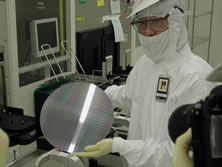
SANTA CLARA, Calif., Jan. 27, 2007 – In one of the biggest advancements in fundamental transistor design, Intel Corporation today revealed that it is using two dramatically new materials to build the insulating walls and switching gates of its 45 nanometer (nm) transistors. Hundreds of millions of these microscopic transistors – or switches – will be inside the next generation Intel® Core™ 2 Duo, Intel Core 2 Quad and Xeon® families of multi-core processors. The company also said it has five early-version products up and running — the first of fifteen 45nm processor products planned from Intel.
 The transistor feat allows the company to continue delivering record-breaking
PC, laptop and server processor speeds, while reducing the amount of electrical
leakage from transistors that can hamper chip and PC design, size, power
consumption, noise and costs. It also ensures Moore's Law, a
high-tech industry axiom that transistor counts double about every two years,
thrives well into the next decade.
The transistor feat allows the company to continue delivering record-breaking
PC, laptop and server processor speeds, while reducing the amount of electrical
leakage from transistors that can hamper chip and PC design, size, power
consumption, noise and costs. It also ensures Moore's Law, a
high-tech industry axiom that transistor counts double about every two years,
thrives well into the next decade.
Intel believes it has extended its lead of more than a year over the rest of the semiconductor industry with the first working 45nm processors of its next-generation 45nm family of products – codenamed ‘Penryn‘. The early versions, which will be targeted at five different computer market segments, are running Windows* Vista*, Mac OS X*, Windows* XP and Linux operating systems, as well as various applications. The company remains on track for 45nm production in the second half of this year.
Intel's Transistors Get a ‘High-k and Metal Gate’ Make-Over at 45nm
Intel is the first to implement an innovative combination of new materials that drastically reduces transistor leakage and increases performance in its 45nm process technology. The company will use a new material with a property called high-k, for the transistor gate dielectric, and a new combination of metal materials for the transistor gate electrode.
‘The implementation of high-k and metal materials marks the biggest change in transistor technology since the introduction of polysilicon gate MOS transistors in the late 1960s,’ said Intel Co-Founder Gordon Moore.
Transistors are tiny switches that process the ones and zeroes of the digital world. The gate turns the transistor on and off and the gate dielectric is an insulator underneath it that separates it from the channel where current flows. The combination of the metal gates and the high-k gate dielectric leads to transistors with very low current leakage and record high performance.
‘As more and more transistors are packed onto a single piece of silicon, the industry continues to research current leakage reduction solutions,’ said Mark Bohr, Intel senior fellow. ‘Meanwhile our engineers and designers have achieved a remarkable accomplishment that ensures the leadership of Intel products and innovation. Our implementation of novel high-k and metal gate transistors for our 45nm process technology will help Intel deliver even faster, more energy efficient multi-core products that build upon our successful Intel Core 2 and Xeon family of processors, and extend Moore's Law well into the next decade.’
For comparison, approximately 400 of Intel's 45nm transistors could fit on the surface of a single human red blood cell. Just a decade ago, the state-of-the-art process technology was 250nm, meaning transistor dimensions were approximately 5.5 times the size and 30 times the area of the technology announced today by Intel.
 As the number of transistors on a chip roughly doubles every
two years in accordance with Moore's Law, Intel is able to innovate and
integrate, adding more features and computing processing cores, increasing
performance, and decreasing manufacturing costs and cost per transistor. To
maintain this pace of innovation, transistors must continue to shrink to
ever-smaller sizes. However, using current materials, the ability to shrink
transistors is reaching fundamental limits because of increased power and heat
issues that develop as feature sizes reach atomic levels. As a result,
implementing new materials is imperative to the future of Moore's Law and the
economics of the information age.
As the number of transistors on a chip roughly doubles every
two years in accordance with Moore's Law, Intel is able to innovate and
integrate, adding more features and computing processing cores, increasing
performance, and decreasing manufacturing costs and cost per transistor. To
maintain this pace of innovation, transistors must continue to shrink to
ever-smaller sizes. However, using current materials, the ability to shrink
transistors is reaching fundamental limits because of increased power and heat
issues that develop as feature sizes reach atomic levels. As a result,
implementing new materials is imperative to the future of Moore's Law and the
economics of the information age.
Intel's High-k, Metal Gate Recipe for 45nm Process Technology
Silicon dioxide has been used to make the transistor gate dielectric for more than 40 years because of its manufacturability and ability to deliver continued transistor performance improvements as it has been made ever thinner. Intel has successfully shrunk the silicon dioxide gate dielectric to as little as 1.2nm thick – equal to five atomic layers – on our previous 65nm process technology, but the continued shrinking has led to increased current leakage through the gate dielectric, resulting in wasted electric current and unnecessary heat.
Transistor gate leakage associated with the ever-thinning silicon dioxide gate dielectric is recognized by the industry as one of the most formidable technical challenges facing Moore's Law. To solve this critical issue, Intel replaced the silicon dioxide with a thicker hafnium-based high-k material in the gate dielectric, reducing leakage by more than 10 times compared to the silicon dioxide used for more than four decades.
Because the high-k gate dielectric is not compatible with today's silicon gate electrode, the second part of Intel's 45nm transistor material recipe is the development of new metal gate materials. While the specific metals that Intel uses remains secret, the company will use a combination of different metal materials for the transistor gate electrodes.
 The combination of the high-k gate dielectric with the metal gate for Intel's
45nm process technology provides more than a 20 percent increase in drive
current, or higher transistor performance. Conversely it reduces source-drain
leakage by more than five times, thus improving the energy efficiency of the
transistor.
The combination of the high-k gate dielectric with the metal gate for Intel's
45nm process technology provides more than a 20 percent increase in drive
current, or higher transistor performance. Conversely it reduces source-drain
leakage by more than five times, thus improving the energy efficiency of the
transistor.
Intel's 45nm process technology also improves transistor density by approximately two times that of the previous generation, allowing the company to either increase the overall transistor count or to make processors smaller. Because the 45nm transistors are smaller than the previous generation, they take less energy to switch on and off, reducing active switching power by approximately 30 percent. Intel will use copper wires with a low-k dielectric for its 45nm interconnects for increased performance and lower power consumption. It will also use innovative design rules and advanced mask techniques to extend the use of 193nm dry lithography to manufacture its 45nm processors because of the cost advantages and high manufacturability it affords.
Penryn Family Will Bring More Energy Efficient Performance
The Penryn family of processors is a derivative of the Intel Core microarchitecture and marks the next step in Intel's rapid cadence of delivering a new process technology and new microarchitecture every other year. The combination of Intel's leading 45nm process technology, high-volume manufacturing capabilities, and leading microarchitecture design enabled the company to already develop its first working 45nm Penryn processors.
The company has more than 15 products based on 45nm in development across desktop, mobile, workstation and enterprise segments. With more than 400 million transistors for dual-core processors and more than 800 million for quad-core, the Penryn family of 45nm processors includes new microarchitecture features for greater performance and power management capabilities, as well as higher core speeds and larger caches. The Penryn family designs also bring approximately 50 new Intel SSE4 instructions that expand capabilities and performance for media and high-performance computing applications.
Intel, the world leader in silicon innovation, develops
technologies, products and initiatives to continually advance how people work
and live. Additional information about Intel is available at www.intel.com/pressroom.
Intel, Core, Xeon and the Intel logo are trademarks or registered trademarks of Intel Corporation or its subsidiaries in the United States and other countries.
* Other names and brands may be claimed as the property of
others.